Internal RAM
My original plan was to use the FPGA for RAM, either by building the RAM in VHDL using flip flops or by using the FPGA’s dedicated RAM blocks.
Building RAM as an array of flip flops worked, but only for small sizes. When I tried to synthesize a 32K version (the minimum amount of RAM the Hack Computer needs) synthesis failed with an error along the lines of too big to synthesize. This was no good.
I then tried using the FPGA’s dedicated RAM blocks and got the following compilation error: Selected device has 26 RAM location(s) of type M4K. However, the current design needs more than 26 to successfully fit.
Interesting. I took a second look at the FPGA’s datasheet…
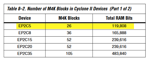
The FPGA I have has 26 M4k blocks. That is, 26 * 4096 bits of memory which is equivalent to 106496 bits of memory. The operating keyword here is bits.
The Hack computer is a 16-bit computer. Each register in memory stores 16-bit values. I had assumed that the FPGA’s internal memory would be more than enough for my needs. 106K was after all way more than the 32K I needed for Hack’s RAM! Except units matter. 106K is in bits, 32K is in registers. At 16 bits per register, 106496 bits yields a measly 6656 registers! This was no good. External RAM it would have to be.
External RAM
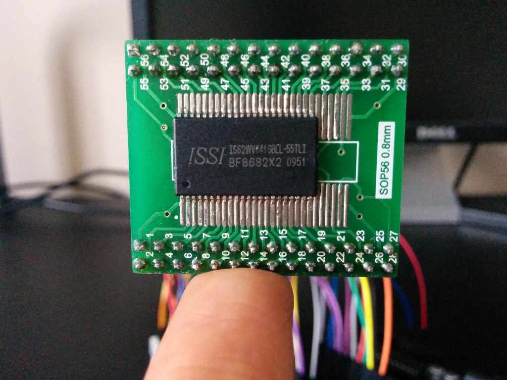
I bought a 64K x 16 bits SRAM. The model number is IS62WV6416BLL and it’s manufactured by ISSI.
Since it comes in a surface mount package, I bought an adapter board from Ebay to break out its pins onto pin headers.
It was my first time soldering a surface mount component. How the RAM still works is beyond me. The amount of heat I exposed it to while trying to solder it onto the adapter board was surreal. A smarter person would have used a non-critical chip to practice with.
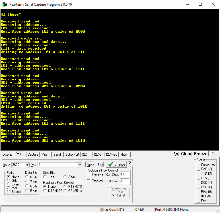
I then set about communicating with the RAM. For this I turned to its datasheet and wrote some Arduino code based on the truth table I found there.
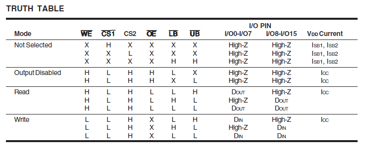
For example, here is the code for the standby, read, and write modes.
void standby() {

    digitalWrite( pin_CS, HIGH );
}

void read() {

    // Set data direction ----
    for( int i = 0; i < nDataPins; i++ ){

        pinMode( dataPins[i], INPUT );
    }

    // Set address ----
    setAddress();

    // Configure for read ----
    digitalWrite( pin_CS, LOW  );
    digitalWrite( pin_WE, HIGH );
    digitalWrite( pin_OE, LOW  );
    digitalWrite( pin_UB, HIGH );  // ignore UB for now
    digitalWrite( pin_LB, LOW  );

    // Read ----
    Serial.print( "Read from address " );
    for( int i = 0; i < nAddressPins; i++ ){

        Serial.print( address[i] );
    }
    Serial.print( " a value of " );
    for( int i = 0; i < nDataPins; i++ ){

        value = digitalRead( dataPins[i] );

        Serial.print( value );
        dataRead[i] = value;
    }
    Serial.println( "\n" );
}

void write() {

    // Set data direction ----
    for( int i = 0; i < nDataPins; i++ ){

        pinMode( dataPins[i], OUTPUT );
    }

    // Set address ----
    setAddress();

    // Configure for write ----
    digitalWrite( pin_CS, LOW  );
    digitalWrite( pin_WE, LOW  );
    digitalWrite( pin_OE, HIGH );
    digitalWrite( pin_UB, HIGH );  // ignore UB for now
    digitalWrite( pin_LB, LOW  );

    // Write ----
    Serial.print( "Writing to address " );
    for( int i = 0; i < nAddressPins; i++ ){

        Serial.print( address[i] );
    }
    Serial.print( " a value of " );
    for( int i = 0; i < nDataPins; i++ ){

        value = dataToWrite[i];

        Serial.print( value );
        digitalWrite( dataPins[i], value );
    }
    Serial.println( "\n" );
}
I noticed timing diagrams in the datasheet but I got away with ignoring them in the Arduino code. However, I won’t have this luxury later when writing the equivalent code in VHDL and timing matters.
The Arduino has 11 digital pins available for use. The SRAM uses 37 pins (16 pins for data, 16 for the address, and 5 for control). To get around this, I connected the five control pins, three data pins, and three address pins to the Arduino. I then connected the remaining data and address pins to ground, effectively setting their values to zero.
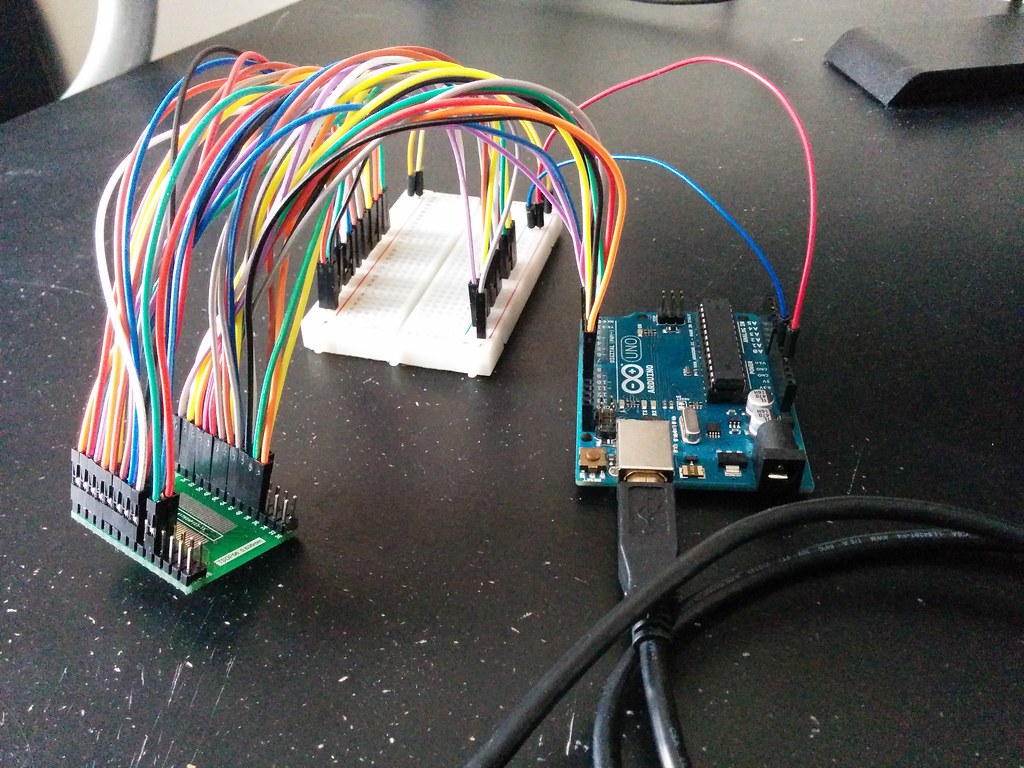
I then uploaded the code onto the Arduino and surprisingly, it worked!
Connecting the 37 wires (plus 4 for power) required by the SRAM was oddly challenging. Also, having the wires all over the place makes everything look complicated, which is completely opposite of the visual aesthetic of simplicity I am seeking. I’ll be keeping an eye out on how to resolve this for the final assembly.
Code