As part of the Homebrew Computer Project, I have been exploring other CPU architectures and their implementations in order to broaden my understanding of CPU design.
An awesome one that I came across was Ben Eater’s 8-bit computer. It is well documented through a series of videos on Youtube and also on his blog. The architecture is simple which allows you to get a firm understanding of all its components.
Since it is a known working design, I saw it as the perfect opportunity to practice implementing a CPU in VHDL.
I started off with some of the code I already had going for the Hack Computer, and added the various elements he implements throughout the series. The resulting code can be found here.
As part of the project, I learned a nifty way to implement ROM. I see myself using something similar for the BIOS the Hack Computer will likely need. Thankfully Ben’s computer does not require a lot of RAM and as such, I could get by using a simple array of registers.
The series helped me gain a stronger understanding of how control logic works to facilitate the execution of an instruction. It was also a good practical exposure to microcode.
Simulation
With the VHDL code sorted out, it was time to simulate! Would it actually work?
I tried some arithmetic code as shown in this video of the series. In the code below, I load the value 5 into register 15, 2 to register 14, and 15 to register 13. I then calculate OUT = M[15] + M[14] - M[13] which should yield -8 (5 + 2 - 15).
// Description:
//  OUT = M[15] + M[14] - M[13]


// Load some values onto ram
LDI 5   // A = X
STA 15  // M[Y] = X

LDI 2   // A = X
STA 14  // M[Y] = X

LDI 15  // A = X
STA 13  // M[Y] = X


// Do the math
LDA 15  // A  = M[15]
ADD 14  // A += M[14]
SUB 13  // A -= M[13]
OUT
HLT
And it worked!
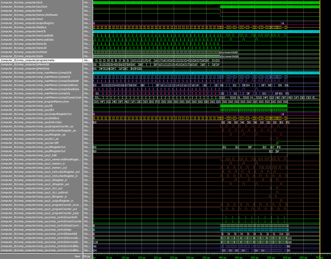
The image is a screenshot of Ben’s CPU executing the above program. (Click on the image to enlarge it). In the image you can see the behaviour over time of various signals of interest such as the databus, current microcode instruction, contents of RAM, control signals such as halt, and the contents of registers such as the instruction, output, and A registers.
The first step of running the program is to upload it into memory. This is accomplished by the procedure below. It is the only non-structural code I use. (Structural code in this case is one that directly maps to a physical implementation of discrete components). Although possible, converting the procedure below to structural code was not a worthwhile endeavor.
architecture ac of computer is

    ...

begin

    ...

    -- Initialize main memory
    comp_st0 : bufferN port map (

        override,                  -- startup control
        memoryNotReady,
        databus
    );
    comp_st1 : mux2to1 port map (

        memLda,                    -- startup control
        memoryAddressRegister_in,  -- runtime control
        memoryNotReady,
        memLoadAddr
    );
    comp_st2 : mux2to1 port map (

        memLdd,                    -- startup control
        memory_in,                 -- runtime control
        memoryNotReady,
        memLoadData
    );

    -- The process below initializes main memory
    --  The process could also be specified at the component level
    --  using flip flops, multiplexers etc. but I'm feeling lazy and
    --  will instead let the synthesis tool come up with whatever
    --  circuitry it wants to accomplish the task.
    process ( clock )
    begin

        if rising_edge( clock ) then

            -- Load programMemory contents onto mainMemory
            if memoryNotReady = '1' then

                case state is

                    -- Hold before going to next
                    when sValid =>

                        memLda <= '0';
                        memLdd <= '0';

                        state <= nxtState;


                    -- Send address
                    when sLoadAddr =>

                        memLda <= '1';
                        memLdd <= '0';

                        override <= pMemAddr;

                        nxtState <= sLoadData;

                        state <= sValid;


                    -- Send data
                    when sLoadData =>

                        memLda <= '0';
                        memLdd <= '1';

                        override <= pMemData;

                        nxtState <= sIncrementAddr;

                        state <= sValid;


                    -- Increment address
                    when sIncrementAddr =>

                        memLda <= '0';
                        memLdd <= '0';


                        if programLineNo < programMemorySize then

                            programLineNo <= programLineNo + 1;

                            pMemAddr <= std_logic_vector( to_unsigned( programLineNo, N ) );

                            nxtState <= sLoadAddr;

                            state <= sValid;

                        else

                            memoryNotReady <= '0';  -- done!

                        end if;


                    -- Should never get here
                    when others =>

                        null;

                end case;

            end if;

        end if;

    end process;

end architecture;
To facilitate this upload, I added a WAIT input signal to the CPU’s design. (It appears as HOLD in the images as they were captured before I renamed it). When WAIT is high, the CPU is suspended. This is accomplished by stopping the CPU’s internal CLOCK signal. While the CPU is suspended, the procedure hijacks the databus to communicate directly with the RAM. It then copies the program code from programMemory into the RAM. Once the procedure has finished the transfer, it pulls the memoryNotReady signal low which then frees the databus and pulls the WAIT signal low which resumes the CPU. You can see all this in the image above (from time 0 to around 380ps).
With the code uploaded to RAM, Ben’s computer happily chugs away and produces the expected result of -8. See the magenta colored output register signal in the image.
The status of some signals (such as the databus) are not clear in the image. This is because I zoomed out to capture the entire duration of the computation. But not to worry, I have created a tutorial on how to run this simulation! After which you can zoom in and out and explore to your heart’s content.
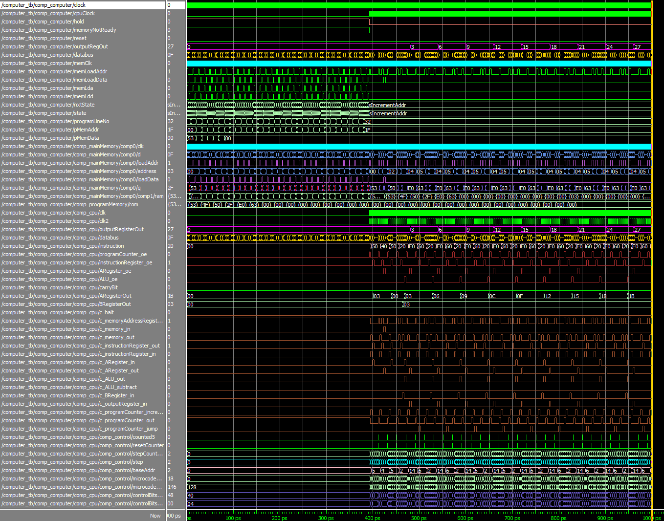
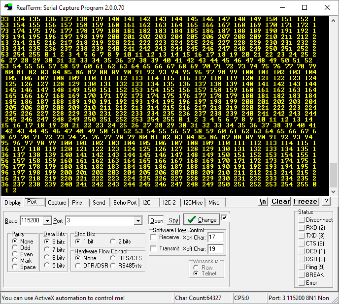
To ensure the computer functioned consistently, I also simulated a second program. This time the ‘add by three’ program shown in this video.
// Description:
//  OUT = multiples of 3

LDI 3
STA 15  // M[15] = 3
LDI 0   // A = 0
ADD 15  // A += M[15]
OUT
JMP 3   // loop indefinitely
And here is a screenshot of the computer executing it,
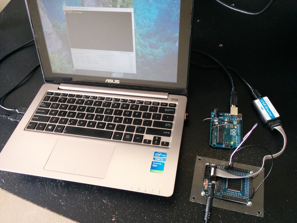
Running on an FPGA
Having the simulation work is great. Having an FPGA configured as Ben’s CPU work would be even better. One key thing had to be sorted before I could do this - how to view the contents of the output register? In the video series, Ben uses a seven segment display to do so. I did not have one on hand, but I did have a PC. Given my earlier experiment with UART, I opted to create a UART interface and use my PC as the display.
I used the awesome Nandland’s UART code as a starting point. I implemented only the transmit half of UART seeing as the CPU’s architecture (at the time of this writing) had no way of receiving data from external devices.
Implementing the UART was not as straightforward as I had anticipated. I will spare you the gory details and talk instead of key events.
The first challenge was getting the UART to successfully send all the data it was meant to send. The UART is configured for a baud rate of 115200 Hz (which is relatively fast among the standard baud rates). The CPU (when configured onto the FPGA) would be running at a clock frequency of 25 MHz. This meant that in the time it took the UART to successfully to transmit a byte of data, the CPU would have performed several additional calculations whose output would be missed. The image below is a simulation of this (while running the add by three program).
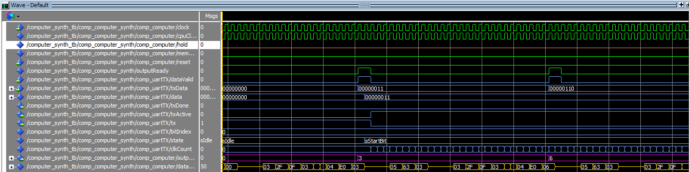
In the image, you can see that in the time it takes the UART to transmit the first bit of the byte of data, the computer has already computed the next value (6). Consider that the UART still has to transmit the remaining seven bits plus a stop bit. By the time it is ready to transmit the next data value, the computer’s output register will hold a value much larger than 6.
To resolve this, I used the WAIT signal described earlier. When the UART is active (as indicated by the txActive signal), the WAIT signal is pulled high which in turn suspends the CPU. When the UART is done transmitting the data, it pulls txActive low which then pulls WAIT low which in turn causes the CPU to resume.
If your PC handled IO this way (halting its CPU until it heard back from an IO device such as a mouse or a WiFi controller), well there would be many a computers with broken screens. However for the purposes of testing whether the CPU was alive, this was a compromise I could live with.
I did try using buffers to capture the missed data and avoid having to suspend the CPU. Unfortunately I can’t remember why that didn’t work out. I suspect it had something to do with figuring out how to trigger the buffer’s read and write signals.
By using WAIT, I managed to get the UART transmitting all the data it needed to. At least in simulation. It was time to configure the FPGA.
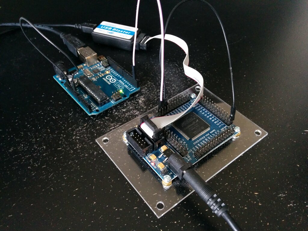
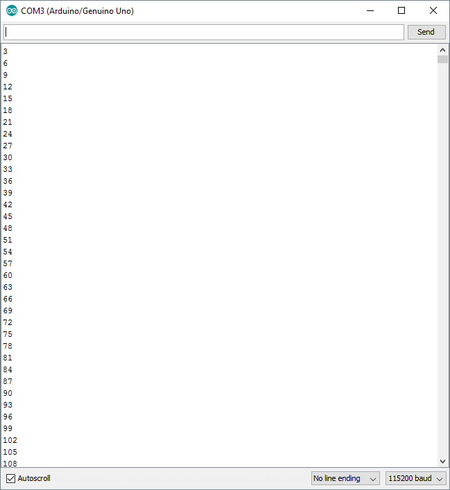
I wired everything up and configured the FPGA with the VHDL code. I then used the Arduino sketch I wrote earlier to see what the FPGA was transmitting. And alive! It was alive and working!
But then I continued watching its output. Over time it no longer seemed to be adding three.
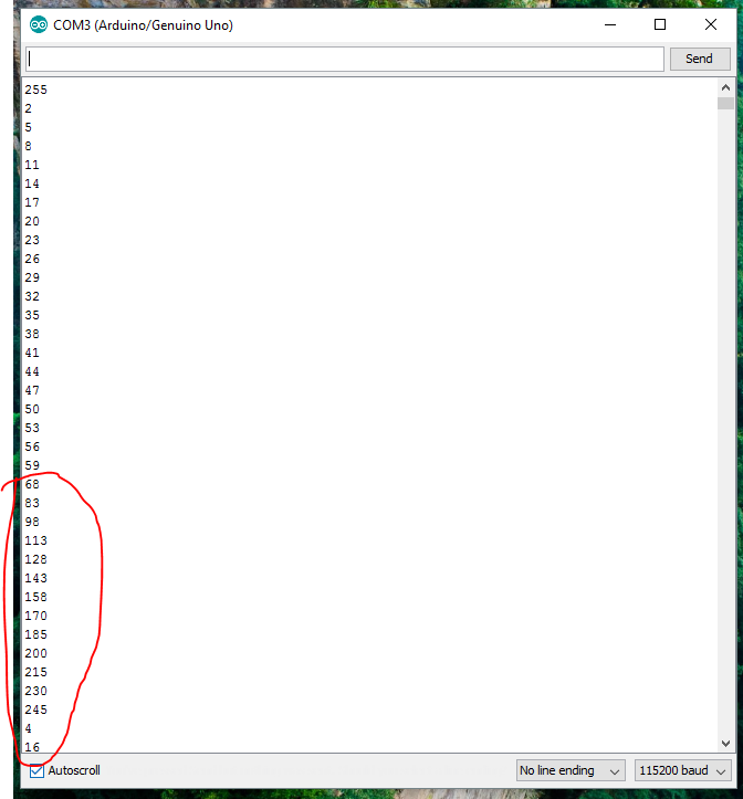
At this point we will fast forward a lot of troubleshooting. For the longest time I thought the problem was with my UART code and that it was somehow dropping packets. I spent more time than I care to admit following this path until I came to the conclusion that there was no way my code was at fault.
I started suspecting the Arduino code, and spent some more time than I care to admit on this path. At some point I was a mouse click away from ordering an FTDI cable and bypassing the Arduino all together. But being the eternal cheapie that I am, I gave Google one more shot. This is when I came across this article by Sudar Muthu describing how to bypass the Arduino’s microprocessor and communicate directly with its FTDI chip. I tried it out, and it worked! The Arduino code acting as a middleman had been the cause of the dropped packets.
The program in the image counts by one. (I had changed it from counting three to simplify debugging).
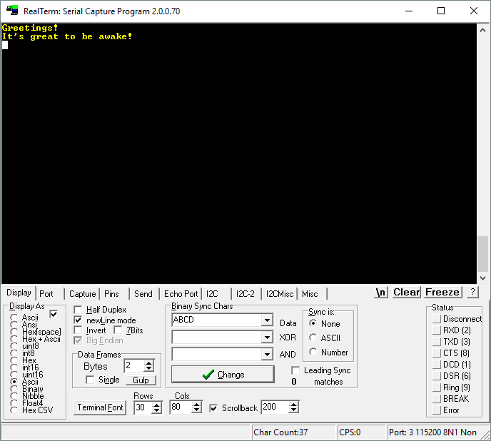
Hello World
With the computer verified working, it was time for a proper hello world. Here is the program I wrote:
// Description:
//  OUT = Greetings!\nIt's great to be awake!\n\n

// G -> 71
LDI 15
ADI 15
ADI 15
ADI 15
ADI 11
OUT

// r -> 114
LDI 15
ADI 15
ADI 15
ADI 15
ADI 15
ADI 15
ADI 15
ADI 9
OUT

// e -> 101
LDI 15
ADI 15
ADI 15
ADI 15
ADI 15
ADI 15
ADI 11
OUT

// e -> 101
LDI 15
ADI 15
ADI 15
ADI 15
ADI 15
ADI 15
ADI 11
OUT

// t -> 116
LDI 15
ADI 15
ADI 15
ADI 15
ADI 15
ADI 15
ADI 15
ADI 11
OUT

// i -> 105
LDI 15
ADI 15
ADI 15
ADI 15
ADI 15
ADI 15
ADI 15
ADI 0
OUT

// n -> 110
LDI 15
ADI 15
ADI 15
ADI 15
ADI 15
ADI 15
ADI 15
ADI 5
OUT

// g -> 103
LDI 15
ADI 15
ADI 15
ADI 15
ADI 15
ADI 15
ADI 13
OUT

// s -> 115
LDI 15
ADI 15
ADI 15
ADI 15
ADI 15
ADI 15
ADI 15
ADI 10
OUT

// ! -> 33
LDI 15
ADI 15
ADI 3
OUT

// \n -> 10
LDI 10
OUT

// I -> 73
LDI 15
ADI 15
ADI 15
ADI 15
ADI 13
OUT

// t -> 116
LDI 15
ADI 15
ADI 15
ADI 15
ADI 15
ADI 15
ADI 15
ADI 11
OUT

// ' -> 39
LDI 15
ADI 15
ADI 9
OUT

// s -> 115
LDI 15
ADI 15
ADI 15
ADI 15
ADI 15
ADI 15
ADI 15
ADI 10
OUT

//   -> 32
LDI 15
ADI 15
ADI 2
OUT

// g -> 103
LDI 15
ADI 15
ADI 15
ADI 15
ADI 15
ADI 15
ADI 13
OUT

// r -> 114
LDI 15
ADI 15
ADI 15
ADI 15
ADI 15
ADI 15
ADI 15
ADI 9
OUT

// e -> 101
LDI 15
ADI 15
ADI 15
ADI 15
ADI 15
ADI 15
ADI 11
OUT

// a -> 97
LDI 15
ADI 15
ADI 15
ADI 15
ADI 15
ADI 15
ADI 7
OUT

// t -> 116
LDI 15
ADI 15
ADI 15
ADI 15
ADI 15
ADI 15
ADI 15
ADI 11
OUT

//   -> 32
LDI 15
ADI 15
ADI 2
OUT

// t -> 116
LDI 15
ADI 15
ADI 15
ADI 15
ADI 15
ADI 15
ADI 15
ADI 11
OUT

// o -> 111
LDI 15
ADI 15
ADI 15
ADI 15
ADI 15
ADI 15
ADI 15
ADI 6
OUT

//   -> 32
LDI 15
ADI 15
ADI 2
OUT

// b -> 98
LDI 15
ADI 15
ADI 15
ADI 15
ADI 15
ADI 15
ADI 8
OUT

// e -> 101
LDI 15
ADI 15
ADI 15
ADI 15
ADI 15
ADI 15
ADI 11
OUT

//   -> 32
LDI 15
ADI 15
ADI 2
OUT

// a -> 97
LDI 15
ADI 15
ADI 15
ADI 15
ADI 15
ADI 15
ADI 7
OUT

// w -> 119
LDI 15
ADI 15
ADI 15
ADI 15
ADI 15
ADI 15
ADI 15
ADI 14
OUT

// a -> 97
LDI 15
ADI 15
ADI 15
ADI 15
ADI 15
ADI 15
ADI 7
OUT

// k -> 107
LDI 15
ADI 15
ADI 15
ADI 15
ADI 15
ADI 15
ADI 15
ADI 2
OUT

// e -> 101
LDI 15
ADI 15
ADI 15
ADI 15
ADI 15
ADI 15
ADI 11
OUT

// ! -> 33
LDI 15
ADI 15
ADI 3
OUT

// \n -> 10
LDI 10
OUT

// \n -> 10
LDI 10
OUT

HLT
I added a custom instruction ADI (which adds the immediate to the accumulator) to facilitate this. As Ben’s CPU is a work in progress at the time of this writing, this instruction had yet to be implemented officially.
And voila!
Takeaways
Simulation in FPGA design is key! If you can get your project to work as desired in simulation, half the battle has been won.
CPU Specs
- Clock speed
- The CPU is running at 25 MHz
- The UART and RAM are running at 50MHz
- Both clock frequencies are limited only by the oscillator I had (50 MHz) and the fact that I did not want to use any IP (intellectual property) cores to multiply it. The clock frequency can be as high as the FPGA you are using supports.
- Everything else (such as RAM size, number of bits, IO interfaces) is configurable with a text editor. That is the beauty of an FPGA design.
Links
Update (May 2018):
Ben added conditional jumps (via zero and carry flags)! The VHDL code has been updated accordingly.